Background
The Ion and Electron Sensor (IES) was launched in 2004 and was flown successfully on the European Space Agency’s Rosetta mission to comet 67P/Churyumov-Gerasimenko. IES made simultaneous measurements of ions’ and electrons’ energies and angular distributions with a wide field of view. IES was a very low-resource instrument, requiring low power, low mass, and a low volume, thus making it highly desirable for missions that require space plasma measurements.
An IES-like instrument has been included as part of the payload in proposals for several new missions led by both SwRI and other institutions. Recently, a dual-ion IES-like variant instrument called the Solar Wind Plasma Sensor (SWiPS) was awarded on NASA’s Solar Wind Follow On at L1 (SWFO-L1) mission. Additionally, another IES-like instrument is now under a Phase A study for potential award on the Solar-Terrestrial Observer for Reconnection in the Magnetosphere (STORM) mission.
Since IES was designed and built over 16 years ago, most of its electronic components have become obsolete. Additionally, better methods for implementing some of the instrument’s functionality have been developed over this time. For the proposals submitted, we took the approach of using flight heritage from portions of multiple other instruments to piece together an electronics package that would make the new version of the IES functional. In theory, this approach will work, but even those heritage circuits would require some modification and revision for the new application, thus reducing their Technology Readiness Level (TRL) from a 9 to a 6 or lower. We felt that the right approach was to completely redesign its electronics package and that is why we proposed this research.
Approach
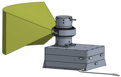 Figure 1: The revised Ion and Electron Sensor instrument proposed for SWiPS.
 In Phase I of this project, our objective was to redesign all electronic circuits and prototype key elements using innovative techniques while at the same time keeping the goals of low power consumption, reduced parts count, and application flexibility in mind. We successfully completed Phase I and were awarded Phase II follow-on funding to build and test engineering models of the various Instrument subsystems to bring the subsystems up to TRL6. Our design approach is based on exploiting the capabilities of modern, high-gate-count, field-programmable gate arrays (FPGA) to the maximum extent possible and designing for low power operation by
- Operating the entire instrument using a single FPGA.
- Implementing a digital feedback control loop and pulse width modulation (PWM) to control all high voltages using high voltage optocouplers.
- Using delay line anodes and pipelined time-to-digital conversion modules to allow finer angular resolution and higher count rates with less parts.
- Using gallium nitride (GaN) field effect transistors wherever possible for inherent radiation tolerance and higher power switching efficiencies.
- Operating the instrument electronics suite from a single ±5V DC-DC converter and voltage regulators for improved overall power efficiency.
- Using a stacked-header board interconnection scheme and an integrated PCB and enclosure slice design in order to eliminate the need for a backplane.
Accomplishments
This project is ongoing. Phase II has built upon the accomplishments of Phase I and to date we have
- Conducted several mechanical peer reviews of the IES sensor design and made minor improvements based on lessons learned, new design practices, and materials changes. The revised sensor design will soon be in fabrication.
- Held several reviews with the microchannel plate (MCP) vendor and settled on the MCPs to order. This order is currently being processed by Purchasing.
- Designed, conducted peer reviews, performed PCB layout, and procured parts for the digital board. Fabrication of this board is currently in progress.
- Designed, conducted peer reviews, performed PCB layout, and procured parts for the low-voltage power supply board. Fabrication of this board is waiting on final PCB layout changes.
- Designed, conducted peer reviews, and procured parts for the high-voltage power supply board. PCB layout for this board is in progress after which boards will be procured and fabrication will be performed.
- Conducted peer reviews on and performed mechanical design for a stacked header board interconnect scheme with an integrated PCB-electronics box slice structure.