Background
The electrical resistance of a macro-scale object is a well-understood property that depends on the resistivity and length-to-area ratio. At the nano-scale, this behavior breaks down, primarily due to the mean free path for electrons becoming comparable to the object dimensions. For example, a 10 nanometer-wide copper interconnect line has an inherent resistivity that is approximately an order of magnitude larger than that of bulk copper (1.68 micro ohm-cm) according to known literature. At this scale, resistivity is no longer a property of the material, but is dependent on dimensions.
This resistivity trend is due primarily to electron scattering at external surfaces and grain boundaries, which are commonly described by two well-known Fuchs & Shatzkes classical models. These models predict that resistivity can be described as a temperature independent product of bulk resistivity times the mean free path (expressed in nanometers), where the mean free path is the average distance traveled by a moving particle (i.e. electron) between successive collisions, as estimated using density functional numerical methods.
Dimensional dependence of electrical conductors could be suppressed by utilizing materials with very small mean free paths, such as iridium (7.09 nanometers), in place of copper (53.3 nanometers). At the other extreme are the semi-metals such as bismuth, whose mean free path is among the longest at approximately 3.4 micrometers, with estimates ranging from 2 to 4 micrometers. This indicates that interesting electrical behavior could occur in bismuth at much more accessible micron and nano scale dimensions. Bismuth has a bulk resistivity of approximately 129 micro ohm-cm at room temperature.
Recent publications have demonstrated innovative methods of growing nanowire scale filament single crystal samples of bismuth, opening up this material to practical research and applications. Some applications of interest may include field emission tips for electron sources, intense and uniform ultraviolet sources, and industrial processes requiring a glow discharge. Bismuth is also biocompatible and could potentially be used in applications requiring electrical conductors at this scale.
Approach
For this project, our focus was essentially one research element including fabricating nanoscale (100-500 nanometer, pseudo one-dimensional) bismuth single crystal filaments having a uniquely reformed crystallization structure (axial or potentially helical configuration outcomes).
Experimental effort employed the use of a colloidal suspension of very small pure bismuth metal particles admixed within a hot viscous dielectric epoxy-polymer having a low molecular weight matrix at approximately 300 degrees centigrade. The admixture was processed while under the influence of a continuously applied static electric field between an electrode and counter electrode. Our objective was to produce small-scale single crystal filaments. The earliest similar work is available via R. Bourgoin, USPTO 1982.
The purpose of the electric field is to promote a recrystallization scheme using the typical hopper crystal geometry as it is essentially stretched and elongated under the influence of an electric field along the preferred fastest growing outer edge of the material. This project was preceded by IR&D project R8943. Our research element objective did not change. However, the method chosen to form potential filaments was modified.
For this project, the heated configuration included molten bismuth that was submerged below a viscous epoxy layer while the admixture was contained in an aluminum vessel. Electrical continuity was formed between the vessel outer wall (counter electrode) and the electrode (touching the top of the bismuth layer) through the molten bismuth.
Filament formation via electrical continuity is inherently influenced by electro kinetic propagation (induced charge electrophoretic osmosis) of the colloidal bismuth particles entering the field gradient as the bismuth admixture slowly cools below the melt recrystallization temperature. Evidence of a continuous yet small bias current (1milli-amp to 1 micro-amp) established between the two electrodes was required to successfully validate our research element as shown in Figure 1 while the electrode was slowly and continuously pulled (1 to 3 mm per minute) out of the bismuth layer in the presence of the electric field. This modified research element, versus the previous project work, was intended to eliminate agglomeration and settling challenges with the bismuth.
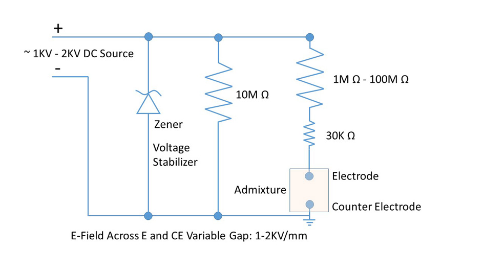
Figure 1: Representative experimental setup (electrical circuit) for recrystallized bismuth.
Accomplishments
Using the aforementioned research element, we were unsuccessful in forming filaments over the short timeframe of this project. Video recordings of several experimental runs did show a temporary bias current between the electrode and counter electrode, indicating potential but brief (several seconds) filament growth. However, these effects were temporary and ultimately were unsuccessful post-process. We believe the electric field orientation and influence may still present unique outcomes for enhancing electrical conductivity of the formed material.