
Background
Switch-mode power supplies (SMPS) have traditionally relied on analog control for its bandwidth, resolution, and low cost, but analog designs suffer from drift, aging, limited modularity, and constraints to classical control theory. Digital control overcomes these issues by offering programmability, reconfigurability without hardware changes, support for multiple loops, and advanced features such as communication and failure prediction, all while reducing board space through integration into microcontrollers or FPGAs. Though challenges remain—such as limited bandwidth, PWM resolution, and processing delays—advances in processors and data converters are addressing these drawbacks. This project aimed to apply secondary side peak-current mode digital control to isolated Low Voltage Power Supply (LVPS) boards, introducing modularity and configurability.
Approach
The research began with the design and simulation of a flyback converter to meet typical LVPS requirements. A traditional analog approach was first implemented for a 28V input and 15V/2A output, using secondary-side regulation, signal isolation through transformers, and continuous conduction mode with peak-current mode control. The system included both an inner and outer loop, with stability and compensation verified before moving to hardware implementation. Once validated, the compensation transfer function was derived and discretized into linear difference equations using the bilinear transform, allowing the design to be transitioned into a digital control architecture where complexity was fixed in code. For digital implementation, the STM32G474RE microcontroller was used, leveraging its Filter Math Accelerator (FMAC) for efficient control loop calculations. Peripherals such as the High-Resolution Timer (HRTIM), ADCs, DMA, and FMAC were configured through STM32CubeMX to handle fast data transfer and real-time signal processing. The digital feedback operated by triggering the internal ADC via the HRTIM to take in a reading and digitizing it. The DMA sends the ADC reading to the FMAC where the FMAC begins calculating the control action through the discrete controller derived. Once the FMAC calculation is complete, the ISR is triggered and a updated duty cycle % is applied to the flyback’s switch. This process then repeats for the next reading. Effectively, what now exists is a digital version of a power supply’s feedback loop that is based on actual derived converter dynamics and models rather than heuristic tuning.
Accomplishments
The PCB was divided into two isolated sections to compare digital and analog feedback, with the digital converter delivering 15V at 2A across a 28–48V input in CCM at ~88% efficiency (83% at half load). The output ripple was only 120mV peak-to-peak, with seamless transition into DCM below 35% load, and the converter maintained stability with a 25dB gain margin and 63° phase margin while showing no overshoot or undershoot under load steps. Finally, ISR and comparator waveforms confirmed no spurious switching events, verifying proper DAC zeroing and adequate slope compensation.
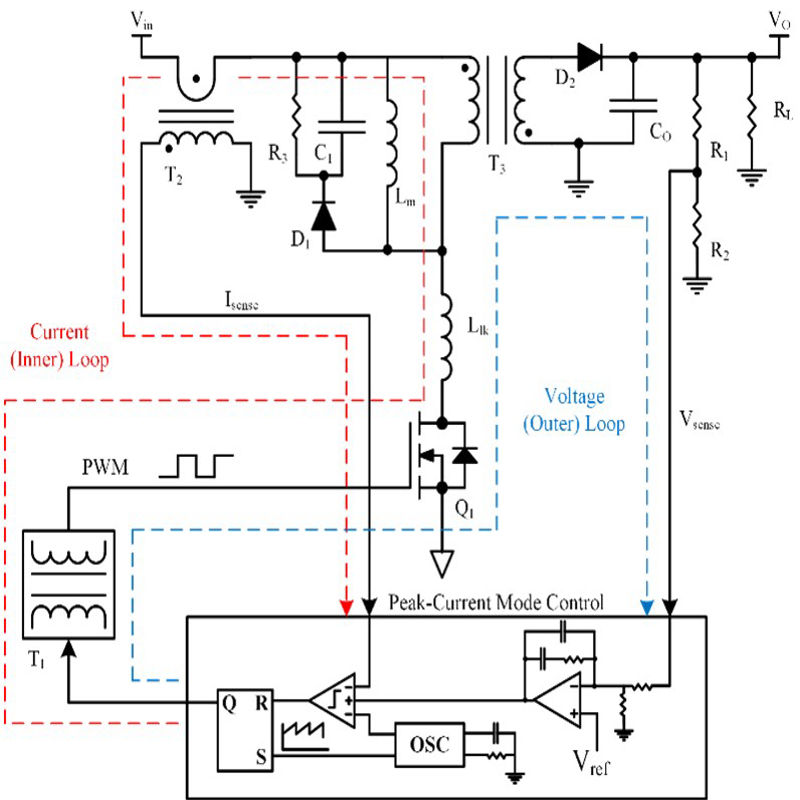
Figure 1: Overall architecture for digital current mode flyback with secondary side regulation.
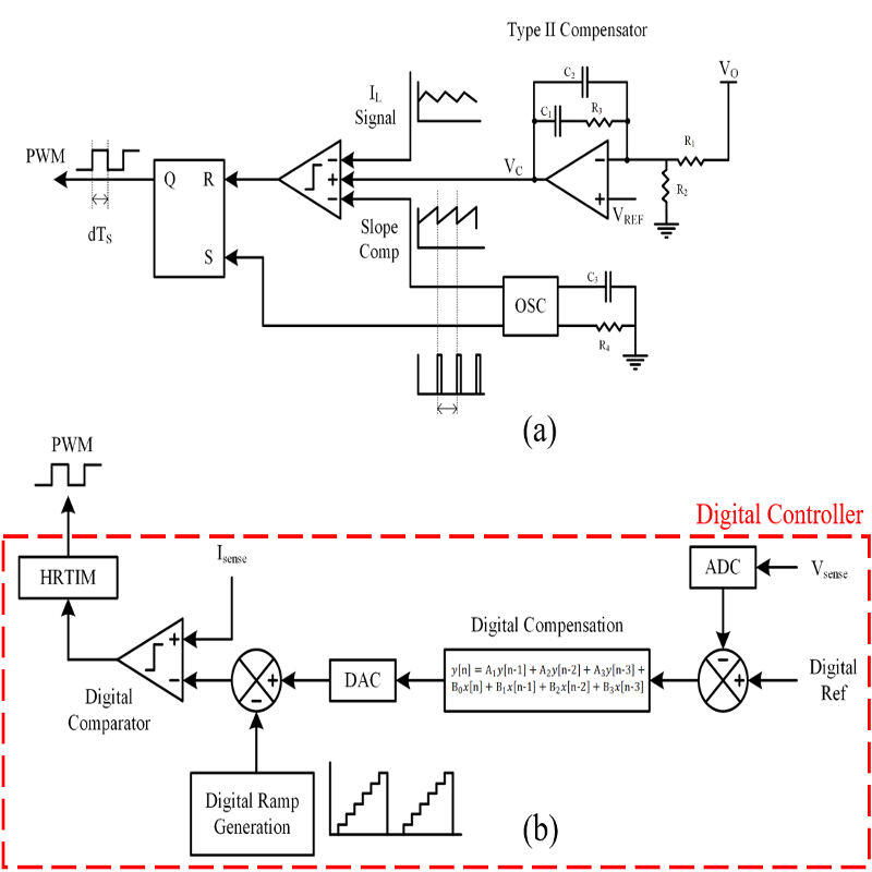
Figure 2: Subfigure (a) shows an analog implementation of a peak-current mode controller with a type II compensator. Note, many of the peripheral components necessary to make the circuit work properly have been excluded. In (b), we have the same control scheme in a digital representation. To clarify, everything within the red dashed box is performed within the processor.
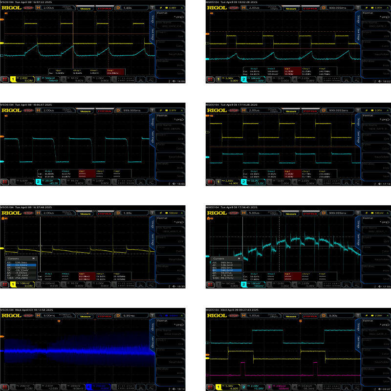
Figure 3: (a) and (b) depict the gate drive (channel 1) and current sense (channel 2) signals at 50% and a 100% load from left to right. Similarly, (c) and (d) show the drain voltage at 50% and a 100% load. These waveforms demonstrate a well clamped continuous conduction mode flyback. Sub-figures (e) and (f) show the output ripple at 50% and a 100% load with the latter having 60Hz sine wave picked up on the scope lead from utility power. (g) is a transient response of 50% load step and is indicative of a well-regulated supply as very little over/undershoot is recorded. (h) shows the gate drive as the yellow trace, the comparator output in the cyan trace, and the ISR routine time in the pink trace.